Thermal imaging
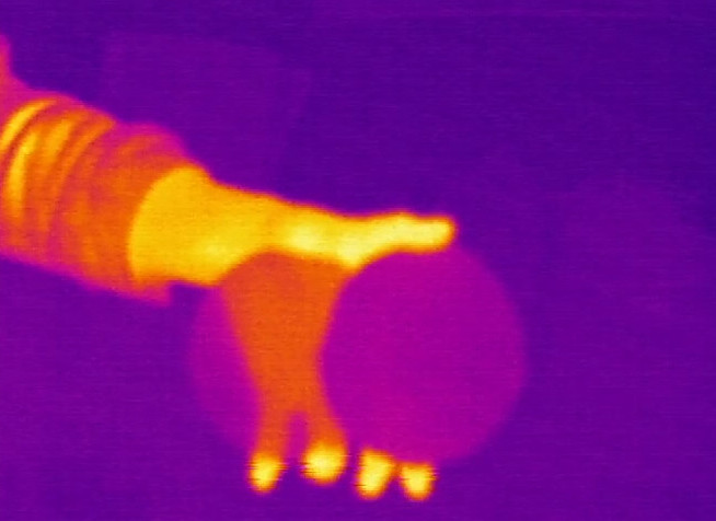
Thermal imaging is a technique to capture the temperature of objects or a scene into an image. The thermal image provides one additional information layer to what can be found in a normal visible image. Benefited from materials science and technology as well as manufacturing advancement, thermal imaging is applied in many fields of daily life:
☛ Distance body temperature monitoring (medical applications)
☛ Early identifying abnormal temperature areas (fire protection)
☛ Enhance a sensing ability of objects in the dark that is applied for self-driving vehicles (automobile)
☛ Enhance security monitoring in remote areas, sea, and islands (security)

Current Thermal Imagers
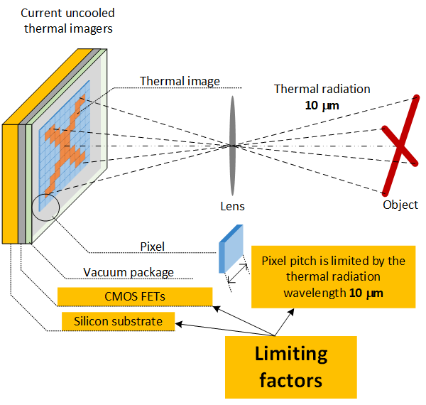
To take thermal images, we need to use thermal chips (as known as imagers/image sensors/focal plane arrays). The most important part of a thermal imager is an active matrix of pixels, normally fabricated on a silicon substrate, which contains an integrated circuit with CMOS field effect transistors, as a base. The principle of thermal imaging of an object, using an un-cooled thermal imager, is the same as that of a conventional digital camera (for example, taken with a camera on a mobile phone). The difference is that the wavelength of thermal radiation is centering around 10 µm, about 20 times longer than that of average visible light.

To be able to obtain a signal from radiation with a wavelength in the range of 10 µm, a minimum pixel size of about 10 x 10 µm² is required. This creates a lower bound for the pixel size. It is the reason that makes the thermal imager not completely suitable for the increasingly smaller manufacturing trend of CMOS technology. Besides, the lower limit makes the size of the whole thermal imaging chip difficult to be small, leading to high production costs, since the latter depends on the total area of the chip. The cost is particularly high for high-resolution thermal imagers. This is a limitation of the nature, which cannot be solved, of thermal imagers when using the monolithic integration with CMOS dies.
Infrasen’s Thermal Imagers
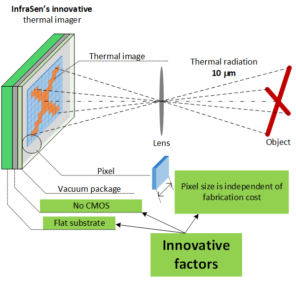
To tackle this inherent problem, Infrasen develops an advanced un-cooled thermal imager that does not use CMOS field effect transistors on the entire area of the thermal imaging pixel matrix.

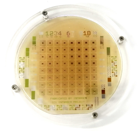
By separating the integrated circuits and sensor matrix fabrication processes, InfraSen’s technology allows components that take advantage of the ever-smaller manufacturing trend of CMOS chips to still be smaller, and components that are lower-bounded in size can still be made larger, without increasing manufacturing costs. Below is a R&D wafer prototype of InfraSen's new innovative imagers

Technological Innovation
InfraSen’s relentless efforts in innovation and improvement in IC design, material fabrication, and microelectromechanical systems (MEMS) manufacturing have enabled InfraSen to build thermal imaging sensors manufacturing technology that minimizes dependence on CMOS ICs.
The difference between the technology developed by InfraSen with current thermal imagers fabrication technology lies in chip design, chip fabrication, and integration of thermal image packaging. These differences create new frontiers for InfraSen’s technology. Below is a short summary
Resolution:
Pixel size:
Frame rate:
Ease of use:
Power consumption:
AI integration:
Affordable:
Portability:
Current imagers
Limited
Tend to be small
Normally 25 Hz
No
High
No
No
No
InfraSen's innovative
Not limited
Not limited
Normally 60 Hz
Yes
Low as mobile
Yes
Yes
Upto terahertz region
Infrasen Thermal Imaging Chip Potential
Removing the tie between the pixel matrix of the thermal imager and the CMOS integrated circuits makes the limit on increasing the resolution of the imager no longer a pure problem of balancing cost and quantity. Moreover, the large pixel size allows the image chip to be more sensitive to external temperature. InfraSen thermal imagers can be manufactured in sufficient quantities and at a minimal cost.
Infrasen technology will enable terahertz thermal imagers fabrication, with radiation wavelength in the range of 100 µm which is hardly possible in a commercializable manner if using current CMOS IC monolithic integration.
Infrasen technology allows the fabrication of thermal imagers on any flat non-conductive substrates that open an integration possibility with flexible electronics for bending thermal imagers generation.
Infrasen technology offers integration with different memristors chip levels; and the potential of having on-chip neuromorphic computational processing.
Infrasen thermal imagers are certainly kept compatible with most popular platforms, such as ARM-based mobile one, with Linux/Android operating systems as well as video processing and AI components in an advanced system-on-chip.